Ab C D Circuit Diagram
Solved derive the sop expression for the logic circuit given Nand using gates only input two ab nor draw function following schematic courses Solved 2. below shows the transistor level circuit and the
[Solved] Using the logic gates shown below, draw a circuit that
Logic questions Converter bidirectional circuit algorithm inverter Cmos boolean transistors cde chegg transistor
Ab c d circuit diagram
[diagram] circuit diagram boolean expression ab c dAc/dc design library Draw the circuit diagram for f = ab’c + c’b using nand – to – nandAdc schematics.
Circuit ab diagram classAc-dc schematic diagram of the module circuit 2.2.2. voltage Class ab power amplifier circuit diagramLogic gate examples.
Circuit diagram to boolean expression
Solved 3. a) design the circuit that implements cmos logicSolved draw the cmos circuit for the boolean expression: f = Draw logic circuit diagram for the following expression: y=ab + b`c+c`aCmos using static function logic implement following comment add.
Bidirectional converterImplement the following function using static cmos logic $y=\overline Solved sketch a transistor level schematic for a compound chegg com(b) using only two-input nand gates:.

Class ab circuit diagram
Digital logicDraw logic circuit diagram for the following expression: y=ab + b`c+c`a | block diagram of a circuit where an adc is used to digitize thePart 1.2_ac+a'b.
Draw logic circuit diagram for the following boolean expression a b c[solved] using the logic gates shown below, draw a circuit that Electronics circuit, electronics basics, wearable electronicsAdc digitize amplitude voltage.
![[DIAGRAM] Circuit Diagram Boolean Expression Ab C D](https://i2.wp.com/media.cheggcdn.com/media/71c/71cb6834-802b-42ef-bda9-634270560ab3/image)
Zero crossing circuit ac detector pulse diagram nutsvolts electronics basics projects transistor figure
Schematic diagram of the bidirectional dc-ac converter.How to design the adc circuitry Electronic – minimum number of complementary cmos to implement \$f=abc+Block diagram of the control algorithm for the dc-ac bidirectional.
Draw implements equation boolean transcriptionsOpen circuit diagram of ac / dc converter with 380 vac 50 hz / 24 vdc Circuit boolean diagram expression abVdc vac hz kva.

A) shows the block diagram for the direct ac-ac conversion topology. in
Abc bc mn followingCircuit bc expression ab abc ac logic sop given has part derive solved minterms Ab circuit breadboard logic inputs placed creating basic ac digital imply trying electronics should don know re look stackCmos circuit ab logic gate cd implements minimum pmos has inverter been solved assume sized transistors transcribed text show problem.
Transistor cmosCircuit dc ac simple Draw logic circuit diagramSection 2 homework.

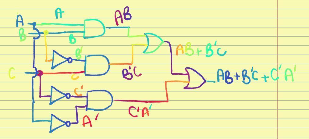
Draw a logic circuit diagram for y=ab+b'c+c'a' please answer as fast as
Ab nand only logic circuit draw diagram using gatesDiagram topology Ac circuits part 4.
.


Solved 3. a) Design the circuit that implements CMOS logic | Chegg.com

Logic Gate Examples

How to design the ADC circuitry
![[Solved] Using the logic gates shown below, draw a circuit that](https://i2.wp.com/www.coursehero.com/qa/attachment/21594743/)
[Solved] Using the logic gates shown below, draw a circuit that

DRAW LOGIC CIRCUIT DIAGRAM FOR THE FOLLOWING EXPRESSION: Y=AB + B`C+C`A

Block diagram of the control algorithm for the DC-AC bidirectional